

Equity X-Ray: In-Depth Research #30a
The Glass Beneath The AI: How a material older than civilization is about to rewire the future of computing

In this new deep research, we’re breaking the topic into 2–3 parts since it’s pretty complex and we want to keep it as digestible as possible.
It’s also something we had to spend time researching ourselves, as it’s not an area where we have deep expertise. Like other topics we’ve covered in recent months such as the space economy (Research #26) or the growing strain on electrical infrastructure from the rise of data centers(Research #27), it starts as a broad idea but can uncover new investable themes.
These themes can help identify publicly traded players positioned to benefit from the trend. In fact, in the second part of the analysis, which we’re aiming to release as early as next week, we’ll highlight at least one listed company that could be a strong opportunity if you believe this theme will play a meaningful role in the future of AI.


WHAT IS A GLASS SUBSTRATE AND WHY SHOULD YOU CARE
Let’s start with something you already know.
You’ve held a smartphone. You’ve watched a video on a laptop. You’ve probably heard that AI is changing everything. But none of that works without a tiny, invisible piece of engineering that sits underneath every chip in every device you’ve ever touched.
It’s called a substrate. And right now, the entire semiconductor industry is in the middle of a quiet revolution about what that substrate should be made of.
For the past 25 years, the answer has been plastic.
Specifically, layers of resin and fiberglass are pressed together into a flat board. Cheap, reliable, good enough. But AI has a way of making “good enough” obsolete very fast.
The Chip Inside Your Chip
To understand why glass substrates matter, you first need to understand what a substrate actually does. Think of it like the foundation of a house. The chip (the processor, the GPU, the memory) is the house itself. The substrate is what it sits on. It delivers power to the chip, connects it to the outside world, and physically holds everything together.
For decades, one chip sat on one substrate. Simple. But then AI came along and completely broke that model.
Here’s the problem: AI models are getting enormous. The number of transistors needed to run something like GPT-4 or the latest NVIDIA Blackwell GPU is staggering. To fit more transistors, chips need to get bigger. But there’s a hard physical ceiling called the reticle limit, roughly 858 square millimeters with current technology. NVIDIA’s GH100 die is already 814 square millimeters. You’re basically at the wall.
And even if you could make chips bigger, you’d run into the yield problem. Imagine drawing a grid on a large canvas. Each square is one chip. Now flick a paintbrush across it. Every square hit by a droplet is defective. The bigger the squares, the more likely each one is to get hit. Bigger chips mean more defects, more waste, more cost.

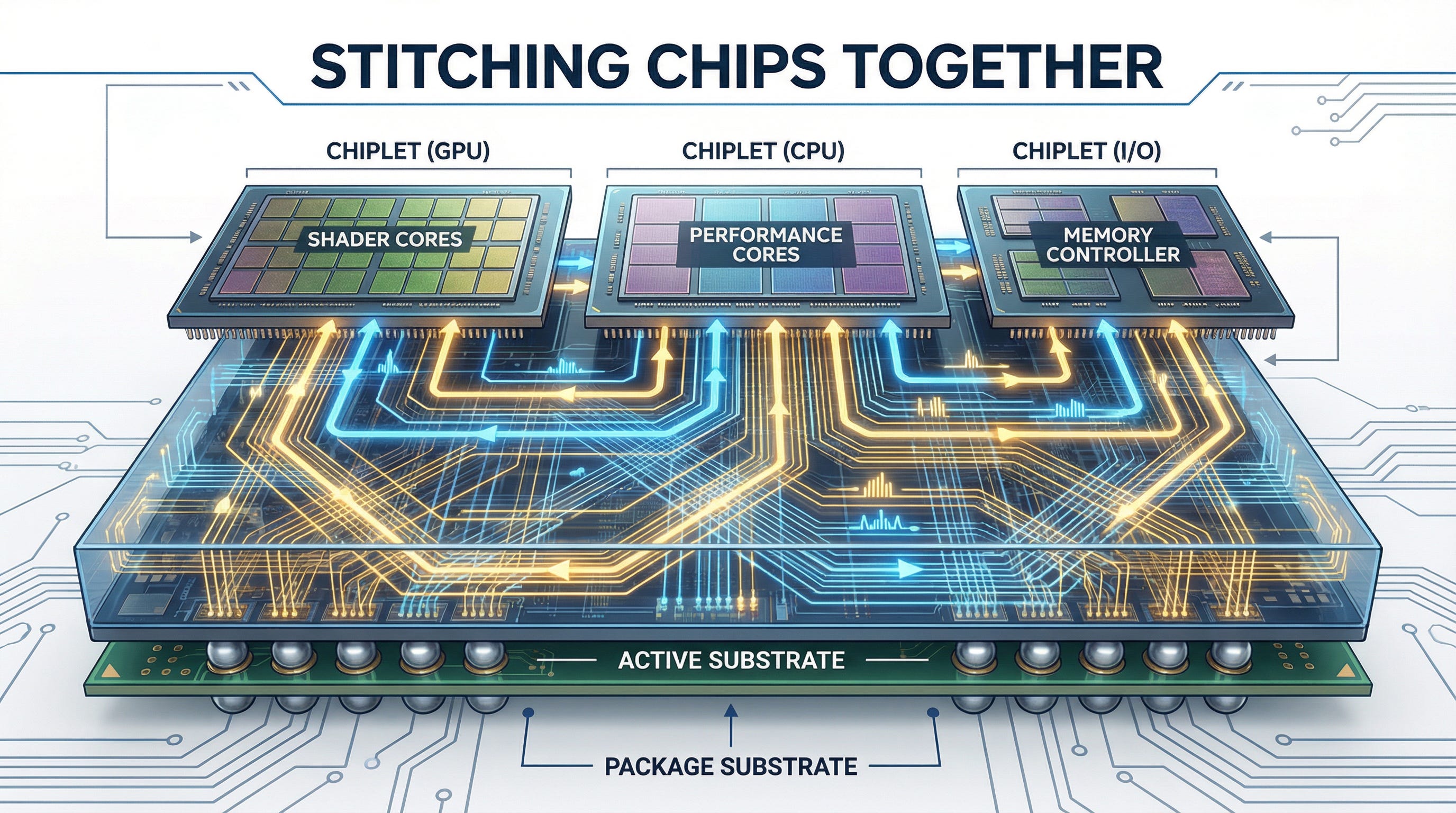
The Lego Revolution: Chiplets
The industry’s answer was chiplets.
Instead of building one massive chip, you build several smaller ones and stitch them together. Think of it like building Hogwarts Castle out of Lego instead of 3D-printing it in one piece. If one brick goes wrong, you swap it out. You don’t throw away the whole castle.
NVIDIA’s Blackwell GPU bonds two near-limit-sized dies into a single processor. Intel’s Ponte Vecchio assembles 47 chiplets into one package. This is the direction the entire industry is moving.
When everything was inside one chip, signals traveled through internal wiring at incredible speed. The moment you split a chip into pieces, those signals have to travel outside the chip to get from one piece to another. It’s like a team that used to work in the same office suddenly scattered across different buildings, forced onto video calls. The quality of those connections determines everything.
This is where the substrate stops being a passive foundation and becomes the most critical piece of engineering in the entire system.
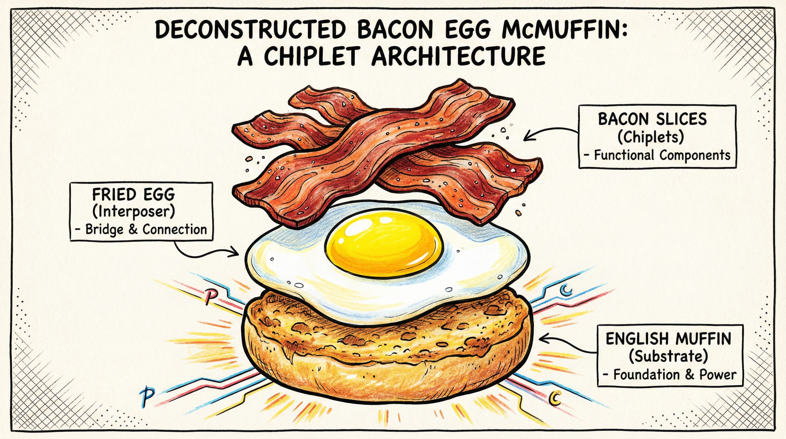
The Bacon Egg McMuffin of Computing
The structure that holds chiplets together looks like a Bacon Egg McMuffin, minus the top bun. Bear with me here because this analogy is genuinely useful.
The English muffin at the bottom is the substrate. It delivers power, connects everything to the outside world, and holds the whole package together. The bacon on top is the chip itself, the GPU, the memory, and the processor. When there was only one chip, you just put the bacon on the muffin and called it a day.
But in the chiplet era, the bacon slices need to talk to each other. So a layer of egg was inserted between the muffin and the bacon: the interposer, a bridge that connects chip to chip at ultra-high speed. This is what TSMC calls CoWoS: Chip-on-Wafer-on-Substrate. C is the chip (bacon), W is the interposer (egg), and S is the substrate (muffin).
The critical question becomes: what do you make the egg and the muffin out of? That decision determines performance, cost, and how many AI chips the world can actually produce.
Why Plastic Is Failing
For 25 years, the substrate (the muffin) has been made of organic material: layers of resin and fiberglass. It worked fine when chips were small and slow.
AI shattered that comfort.
There are two tests a good substrate must pass.
The first is surviving heat. All materials expand when they get hot. When an AI chip burns hundreds of watts, both the chip (silicon) and the substrate beneath it expand, but at different rates. Silicon expands at roughly 3 parts per million per degree Celsius. Organic substrates expand at 17 to 20 parts per million. That’s a six-to-seven-fold difference. For small packages, you could ignore this. For the massive packages that AI chips require, the warping becomes catastrophic. Solder joints crack. Connections fail.
The second test is signal quality. When electrical signals pass through a substrate, the material absorbs some of that signal energy. At the ultra-high frequencies that AI chips demand, the signal gets smeared beyond recognition. Restoring a smeared signal forces the chip to work overtime, consuming more power, generating more heat, which further degrades the signal. A vicious cycle.
Organic substrates passed both tests comfortably for 25 years. In front of AI chips, both tests collapsed simultaneously.
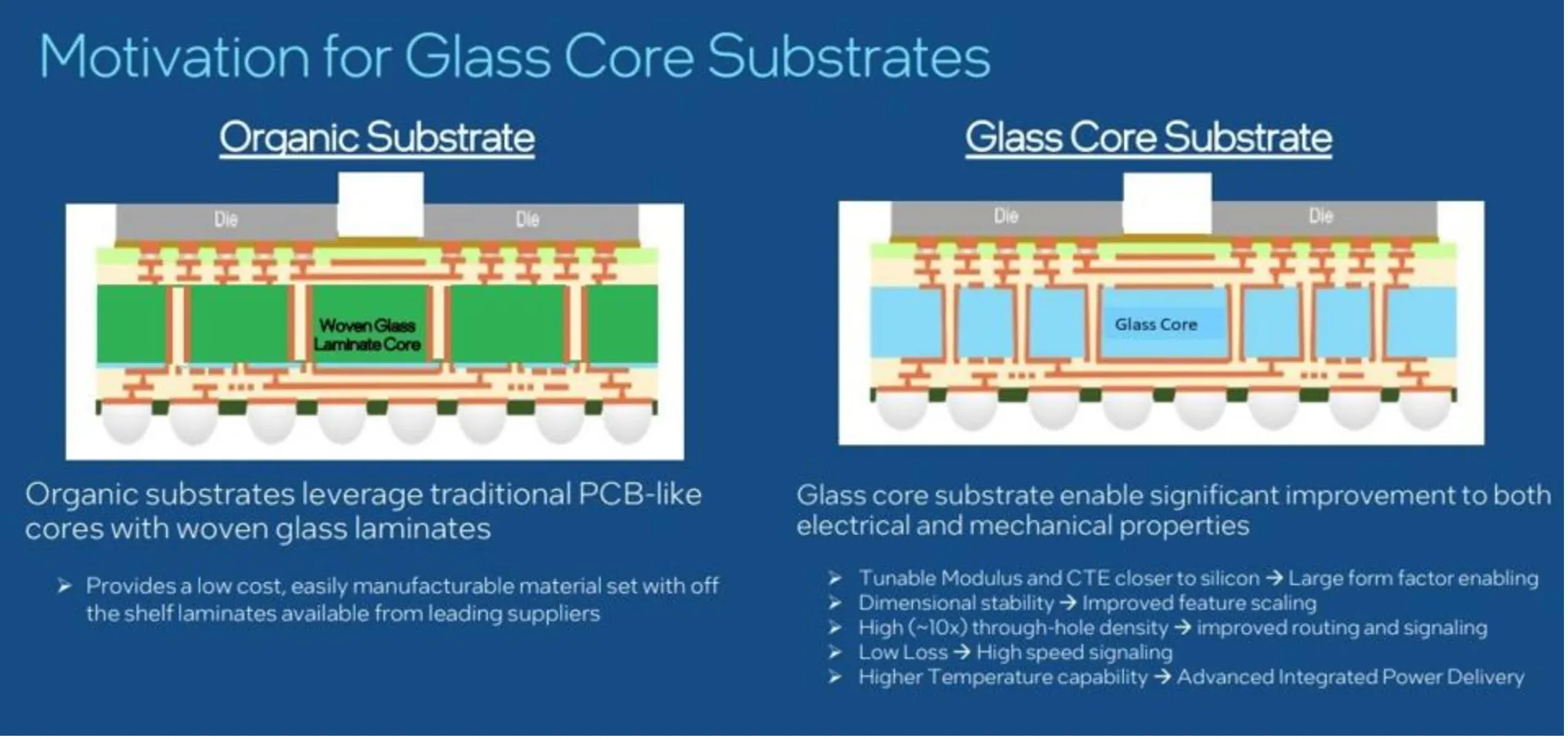
Enter Glass
Glass can be tuned in composition to approach silicon’s thermal expansion rate of 3 parts per million per degree Celsius. That six-to-seven-fold mismatch with organic substrates? Glass eliminates it. Package sizes that are physically impossible on organic substrates become feasible on glass.
On signal quality, glass is even more dramatic. Signal loss through glass can be more than 10 times lower than through organic substrates. Less signal smearing means less burden on recovery circuits, less power consumption, and less heat. The vicious cycle breaks.
But glass has two more properties that organic substrates can never imitate, and these are where things get genuinely exciting.
Glass surfaces are extraordinarily smooth. If an organic substrate’s surface is a dirt road, a glass surface is a skating rink. This smoothness enables a technology called hybrid bonding, where copper pads are pressed directly together without solder. This can shrink the pitch between connection points from tens of micrometers to below 10 micrometers, creating tens of times more connections in the same area. Impossible on organic substrates. Possible on glass.
And glass is transparent. Light passes through it. This means optical waveguides can be embedded directly inside the substrate. The future where electrical signals convert to optical signals and travel between chips at the speed of light? Glass is the material that makes that possible.
The Through-Glass Via: The Hole That Changes Everything
Here’s where it gets technical, but stay with me because this is the crux of the whole story.
A substrate isn’t just a flat piece of material. It needs vertical connections, holes drilled through it that carry signals and power from one layer to another. In organic substrates, these holes are made with lasers. In glass, you need something different because glass is brittle, and lasers can cause micro-cracks.
The solution is called a Through-Glass Via, or TGV. Creating millions of these microscopic holes in glass, filling them with copper, and doing it reliably at an industrial scale is one of the hardest manufacturing challenges in the semiconductor industry right now. It requires specialized wet-process equipment, precision chemistry, and process control that very few companies in the world can provide.
This is not a software problem. This is not a design problem.
This is a physical manufacturing problem. And the companies that solve it first will own a chokepoint in the AI supply chain.
The Honest Challenges
Glass is not a silver bullet. If it were, it would already be everywhere.
Glass breaks. During cutting, drilling, and handling, microscopic cracks form. As a chip powers on and off thousands of times, expanding and contracting with each cycle, those cracks can propagate. The industry is working on edge-finishing techniques and strengthening treatments, but long-term reliability data across thousands of thermal cycles is still being accumulated.
Glass conducts heat poorly, about 100 times worse than silicon. This is a real challenge for thermal management. Interestingly, this weakness partially cancels out if optical interconnects are embedded in the substrate, since light-based signals generate almost no heat. Glass’s weakness and optical interconnects’ strength complement each other in a way that feels almost designed.
And glass is expensive. Mass production yields are still far below organic substrates. Costs run several times higher. The economics gap is real, and it is the primary reason glass hasn’t already taken over.
But here’s the thing about technology transitions: they don’t happen when the new technology is perfect. They happen when the old technology hits a wall that it cannot climb over. Organic substrates are approaching that wall right now.
Disclaimer: This analysis is for informational purposes only and should not be considered financial advice. Always conduct your research and consult with a licensed financial advisor before making investment decisions.